
Hello everyone. Thank you for taking a look. If you ever wanted a fundamental starter guide to start designing your keyboards using KiCad, you have come to the right place. This guide will go over how to make a keyboard, from installing KiCad, all the way down to getting the board manufactured.
I will not be going over setting up the firmware. I will do another writeup on this for both QMK and KMK later.
Definitions
Schematic: A schematic designed with KiCad is more than a simple graphic representation of an electronic device. It is normally the entry point of a development chain that allows for:
- Validating against a set of rules (Electrical Rules Check) to detect errors and omissions.
- Automatically generating a bill of materials.
- Generating a netlist for simulation software such as SPICE.
- Defining a circuit for transferring to PCB layout.
Cite: See KiCad Docs For more information on schematics.
PCB: PCB stands for Printed circuit board. It is the board that holds all of the components/electronics.
Symbol: A symbol is a representation of a footprint within a schematic.
Cite See KiCad Docs For more information on Symbols.
Component: A component is the physical device attached to the PCB. In KiCad, components and symbols are generally referred to as the same thing. This is because older software versions used the word component instead of symbol. Once you know this, it clears up a lot of confusion. For the most part, components made with older software versions can still be used as symbols with newer versions, which is why knowing is essential.
Footprints: A footprint can be defined as the copper connections between physical components and traces on a Circuit board. In other words, it shows up on the physical board.
Cite: See KiCad Docs For more information on footprints.
Downloading KiCad
To start, you should download KiCAD to whatever OS you work from. I will be using Windows for this guide. I will also be using KiCad 7. You are welcome to use whatever version suits you as well. But 7 has legacy support and some quality-of-life improvements that make things easier.
Once the program is installed, go to File -> New Project. Make a name for your project, and save it wherever you want. There should be two files. You can open both, but we will be working out of the <Project Name>.kicad_sch file first.
Importing Footprints and Components
Usually, commonly used footprints and symbols will be in the default global library. Unfortunately, some of the ones you will need for this project must be downloaded and imported. For this project, I will be using this switch library on GitHub. You can download it by pressing Code -> Download ZIP. Extract the file to your project folder. I like to make a new folder and name it something. Footprints folders end in .pretty. If the folder you extracted is called something else, ensure it ends in .pretty.
Example: keyswitches.pretty
To import footprints, go to the main project page and select Preferences -> Manage Footprint Libraries.
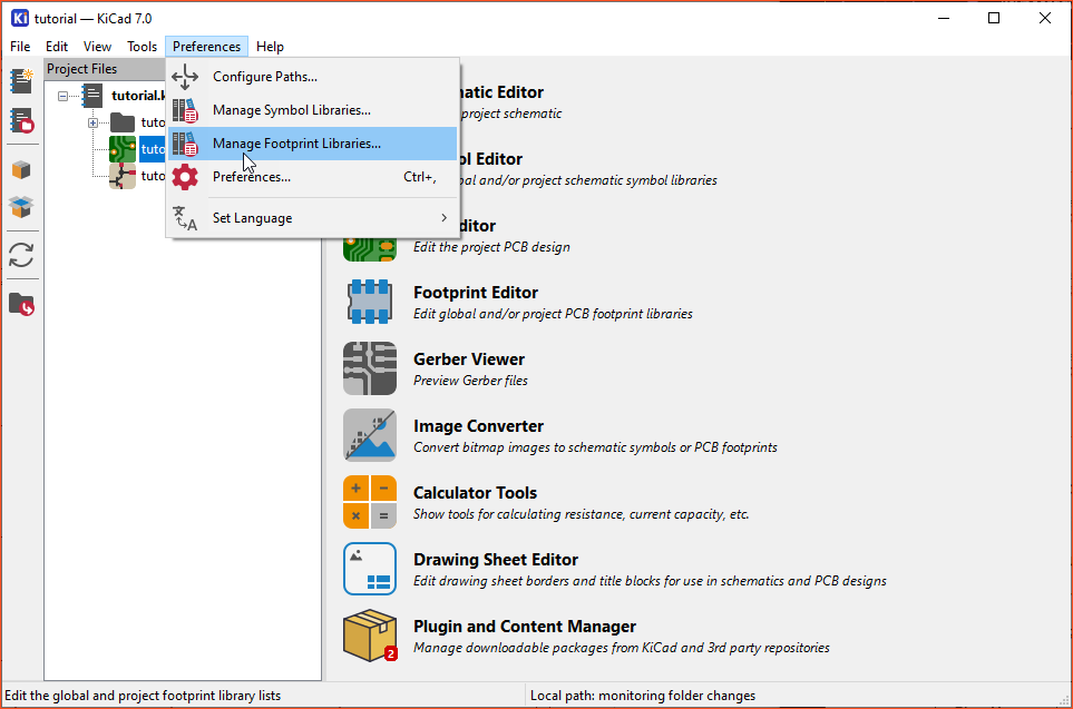
It is up to you if you would prefer to import into the Global Libraries or the Project Specific Libraries. Global means they will show up in every project, whereas project-specific implies that it will only be used for this project.
To import, press the Folder button.

Find the <FolderName>.pretty folder that you want to import, and press. Open.
I will use a Raspberry Pi Pico for this project for my MCU. Download the files the same way that you did above. Once downloaded, find the .pretty folder. Additionally, there will be a .kicad_sym file there. You will want this file as well. Import the <FolderName>.pretty file the same was as above.
To import the .kicad_sym file, you will instead go to Preferences -> Manage Symbol Libraries, select the folder icon again, and then find the file, press Open then OK. It is a similar process.
Adding Components to the Schematic
To add components, press this icon or hit the A key on your keyboard.

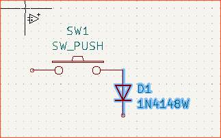
I usually use the SW_Push from the default global symbols library. You can search for it in the search bar. Then, add a diode by searching for 1N4148. For this tutorial, I will be selecting surface mount diodes. So 1N4148W should work fine. The default SOD-123 Footprint should be fine too. Then press OK.
Using the R key on your keyboard, you can rotate any component. The diodes can face either direction. But the default for QMK is facing this direction. Connect the diode to the switch; It should look something like this.
Select the Select tool from the right toolbar.

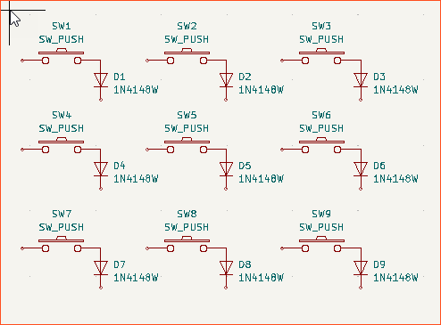
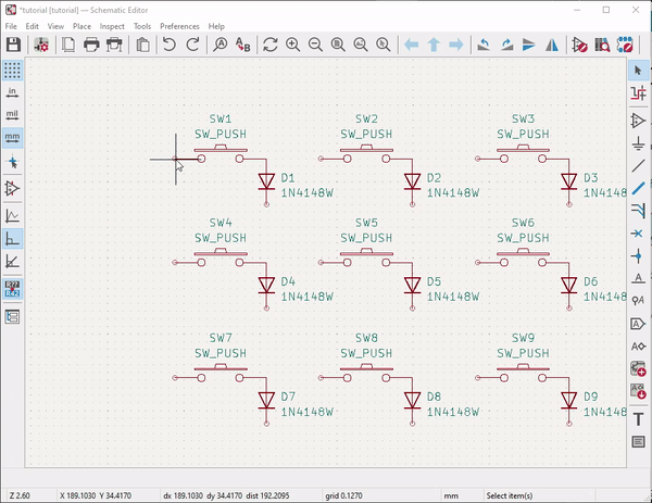
Highlight the switch diode combo you made, and hit CTRL+C on your keyboard to copy it and CTRL+V to paste it. I am going to make a 3×3 keypad for this tutorial. If you need to move anything after placing it, you can highlight the component(s) and use the M key on your keyboard to move them.
When you are done, you should have something like this.
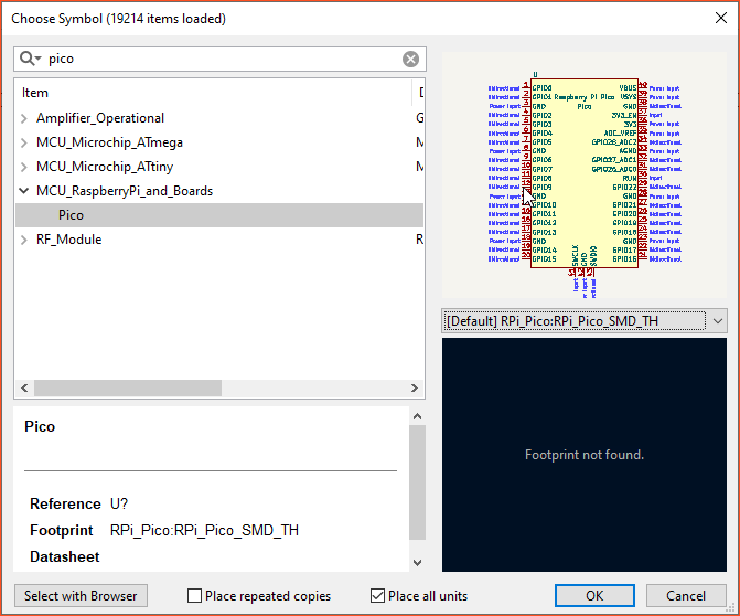
Then, you can add the Raspberry Pi Pico that we imported earlier. Add another component and search for Pico. When you find it, select it and add it to your schematic.
Connecting Everything in the Schematic
There are several ways that we can connect different components. We will usually use a combination of methods.
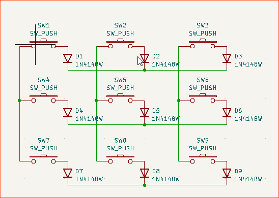
I first like to select the add a wire tool

I begin to wire the rows and columns. It should look something like this.
Once you finish, it should look like this.
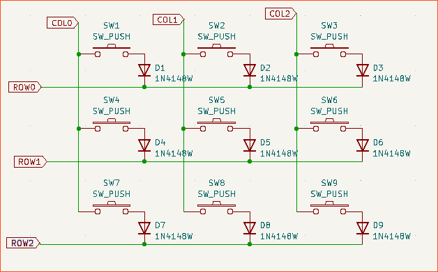
After this, you can use labels to connect each row and column to their respective pins on the MCU. You can almost think of it as a wireless wire.
I will be using Global Labels for this. (NOTE: Using Global labels is not best practice when you get into more complex schematics. Some schematics use multiple sheets. Global labels are a way to connect items between multiple sheets. For the sake of simplicity, I will be using Global labels. But keep this in mind when you are getting into more complex stuff.)
This is the Global Label icon.

Name each row and column using a label. Once you are finished, it should look something like this.
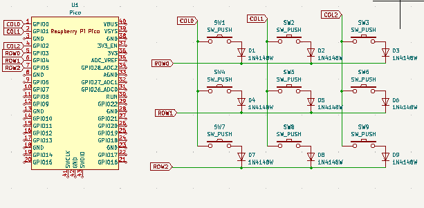
Now, you can add the same labels to the MCU, connecting each row and column to their respective pin on the MCU. Any GPIO Pin will work fine.
Assigning Footprints to Components
Run the footprint assignment tool. It should look like this.

From here, you will have three columns. The one on the left is called Footprint Libraries. The one in the middle is called Symbol: Footprint Assignments, and the one on the right is called Filtered Footprints.
You will want to find the name of your .pretty folder on the left side; select which component you would like to add the footprint to in the middle, then double-click which footprint you want in the right column.
See the below example.
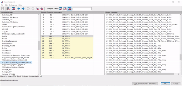
Once you have assigned everything, Click Apply Save Schematic & Continue. Then press OK. Then, we can design the PCB.
(Note: some footprints might already be assigned; as you can see in the video, the diodes are already assigned along with the Pico)
Using the PCB editor
Now that you have created a schematic, you can open the <Filename>.kicad_pcb.
I would highly recommend changing the grid. In the taskbar at the top there will be a dropdown called Grid.

Click on the dropdown and click edit user grid. Set the Size X and Size Y to 0.254, then press OK. Make sure to select it in the dropdown box.
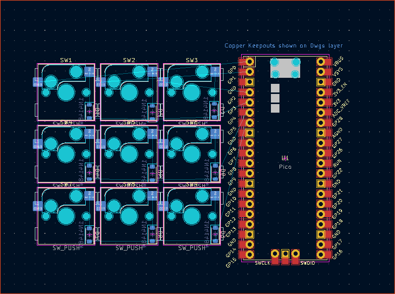
Click the Update PCB Button.

When you get a popup window, press Update PCB. All of your footprints should show up. You can click to place them all down. Then, you can move things around by clicking them and pressing M on your keyboard.
If you want to rotate anything, you can hit SHIFT+M after highlighting the part. If you want to flip anything to the other side of the PCB, you can hit the F key on your keyboard after selecting the part(s).
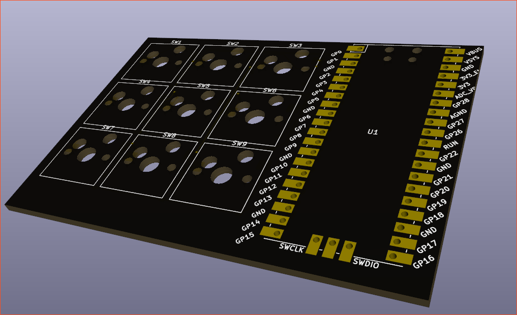
This is what mine looked like when I was finished.
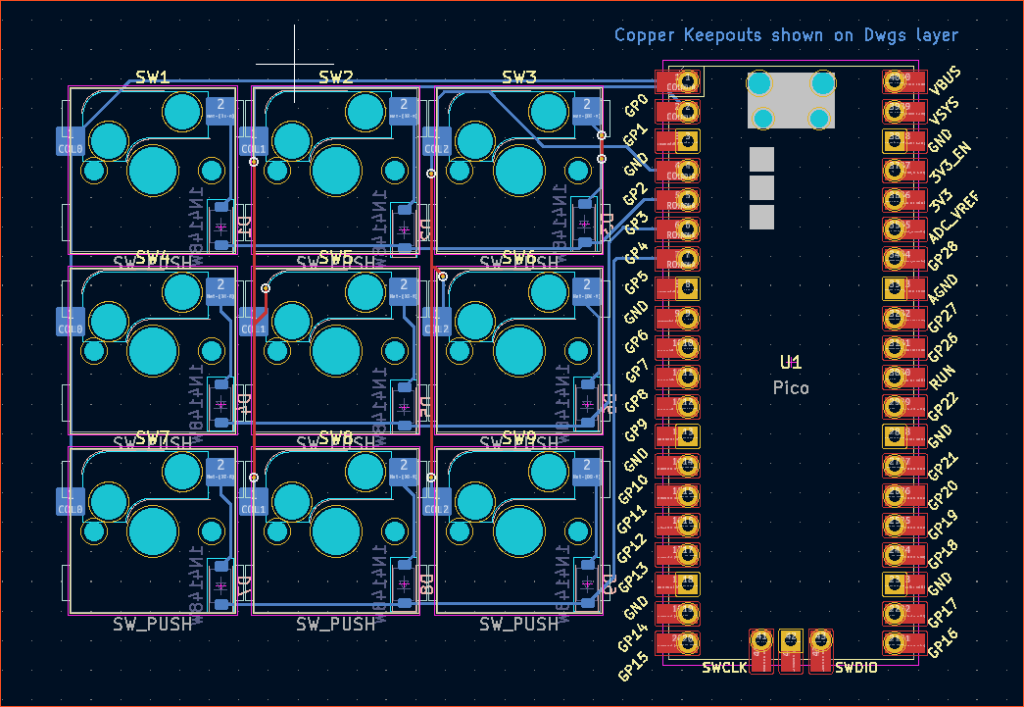
Routing Wire Tracks
To route tracks, you can select the Route Tracks tool.

There is a column on the right-hand side of the page called Appearance, where you can select different board layers. The red and blue are the ones we want to choose. These are the tracks. Red is the top of the board; Blue is the bottom of the board.
Once the route Tracks tool is selected, click on any of the pads.
When a pad is selected, it should highlight the corresponding connection. If it doesn’t show up, it is likely not set up correctly in the schematic.
You can press the V key on your keyboard while routing to create a via. A via is a copper connection from one side of the board to the other. You can use these to route things more efficiently or if you have clearance issues.
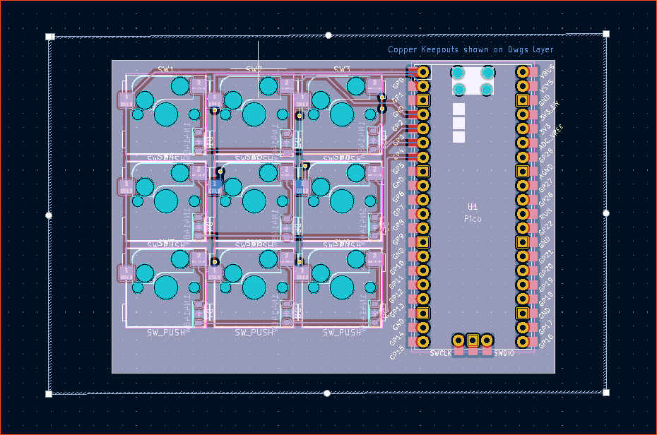
Here is what mine looks like after routing all of the traces.
After you finish routing the tracks, you should make edge cuts. In the Appearance column, you should select the Edge.Cuts layer. From the right toolbar, you can select any of the drawing tools. I will choose the rectangle tool and draw a basic cut for this project. It will look something like this.
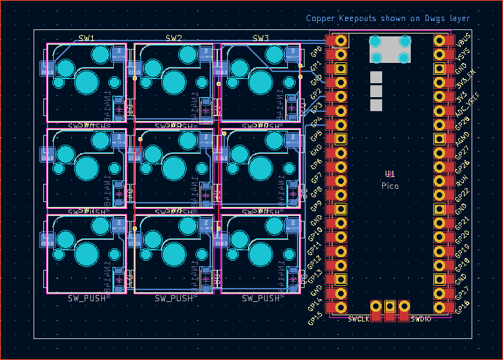
To see how everything turned out, click the View dropdown at the top and select 3D Viewer.
This is what my PCB looks like.
If you are satisfied, you can start to add a fill. A fill fills in all of the copper between the Tracks and Vias. This step isn’t necessary, but I would recommend it.
Select the Fill Tool from the right-hand toolbar, then select the F.Cu or B.CU from the Appearances column.

Then, you can click on the board. It will pull up a new box. You should select both layers in the left-hand column and press OK. (Please make sure <no net> is selected on the right-hand side.)
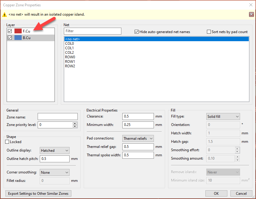
Draw around your PCB. Once the box has been drawn, Press B on your keyboard to build the Fill zones. If you change the board after this, always rebuild the fill zone.
It should look something like this.
Next, you will want to run the DRC tool (Design rule checker.) Press this icon in the top toolbar.

You will get a popup, and then you can press the Run DRC button.
This will give you a list of violations. You will likely get some warnings. Usually, warnings are fine. If you are worried, check them and see what the problem is. You should be on the lookout for Errors, and make sure nothing is showing up in the Unconnected Items Tab.
(Please note that you can add your own custom silkscreens, I will not be going over that in this tutorial. If you would like to learn more, there are some good videos you can watch. I might make a written tutorial on this later.)
Once you are satisfied with everything, you can move on to the next step.
Exporting and manufacturing
I use JLCPCB. It is the cheapest option here in the USA. They already have an excellent write-up on how to export in Kicad. So I will not be going into detail on how to export.
Once you have exported the Gerber and drill files, open the folder that you exported them to.
Select all of the files and zip them into a zip folder.
Once they are zipped, you can head over to JLCPCB. From there, select Order Now from the top menu. You can either drag and drop the zip folder or click Upload Gerber File and find your zip folder.
Make sure everything looks right. You can select how many you want. But all of the defaults should be fine. The only thing I usually change is I use LeadFree. It’s just a couple of cents more.
Follow the prompts to check out, and then you are done!
Thanks so much for this concise write-up! I would love to see you give a similar treatment to the firmware piece and a third tutorial on silkscreen and other cosmetic strategies.
Both of those are in the works! The big one is QMK. I feel like A LOT of people struggle with it. I myself run into issues pretty much every single time I make a new board.